Flip Chip Package
Flip chip interconnect when higher inputoutput IO counts are needed 1 2. Typical Flip-Chip packages The Flip-Chip package family has been designed to fulfill the same quality levels and the same reliability performances as standard semiconductor plastic packages.
 Simplified Cross Section Of A Flip Chip Package Which Is Mounted On Pcb Download Scientific Diagram
The wafer level package flip chip and UCSP represents a unique packaging form factor that might not perform equally to a packaged product through traditional mechanical reliability tests.
Flip chip package. FcFBGA packages are also available in very thin profile hybrid flip chip flip chip on the bottom and wirebond die on the top such as fcTFBGA-SD2 and fcTFBGA-SD3. Micro-bumped flip-chip packages The Flip-Chip package family has been designed to fulfill the same quality levels and the same reliability performances as standard semiconductor plastic packages. AA AA AA AA AA AA AA AA AA FILLET ENCAPSULANT SEMICONDUCTOR CHIP GOLD-TIN SOLDER BUMP CERAMIC CARRIER THICK-FILM PALLADIUM-SILVER METALLIZATION Figure 9-11.
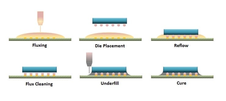
Disposing a stencil on the upper surface of the substrate strip so as forming an air gap between the stencil and the. An essential process for flip chip packaging is wafer bumping. Flip Chip is not a specific package like SOIC or even a package type like BGA.
Crack in BEOL dielectric stacks left not wet bump induced by higher warpage Ref. It considers the effect of bare die or die-size. Flip Chip describes the method of electrically connecting the die to the package carrier.
Utilizing multiple high density routing layers laser drilled blind buried and stacked vias and ultra fine linespace metallization FCBGA substrates have the highest routing density available. Amkor is committed to being the leading provider of Flip Chip in Package FCiP technology. Providing a substrate strip wherein the substrate strip comprises at least one substrate and comprises an upper surface and a lower surface.
To meet the requirement of higher IO counts the flip chip chip scale package fcCSP has become the mainstream package type for mobile application processors AP as well as baseband processors BB 3. Good adhesion between the underfill material the carrier and the chip surface is needed for stress. The packages reliability is integrally linked to the users assembly methods circuit-board material and.
Chip Package Interaction CPI in Flip Chip Package September 13 2020 Resham Thapa Semiconductor Assembly Packaging 0 Chip package interaction CPI is the interaction between semiconductor package stresses and semiconductor devices. This paper provides a comparison of different commonly used technologies including flip-chip chip-size and wafer level array package methodologies detailed in a new publication IPC-7094. Due to the fcCSP features the mobile low power double data rate.
By partnering with proven industry leaders Amkor has brought high volume flip chip packaging and assembly to the subcontract market. The wafer level package flip chip and UCSP represents a unique packaging form factor that might not perform equally to a packaged product through traditional mechanical reliability tests. FCBGA fcLBGA fcLGA FlipStack CSP and fcCSP packages are qualified and in production.
A flip chip package process comprising. The package carrier either substrate or leadframe then provides the connection from the die to the exterior of the package. The packages reliability is integrally linked to the users assembly methods circuit-board material and.
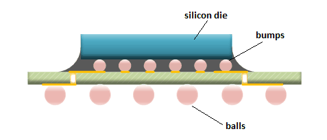
Flip chip technology has its name by flipping over the chip to connect with the substrate. Reflowing packages with flip chip bump interconnects requires a good balance of substrate package material sets and controlled reflow profiles to ensure proper melt of the bump interconnects and solder joint reliability thru subsequent reflow processes at assembly facilities. Flip-chip and incorporating more than one die or more than one part in the assembly process.
Flip chip production capability exists in our Portugal Philippines Korea. Flip chip microelectronic assembly is the direct electrical connection of face-down or flipped integrated circuit IC chips onto substrates circuit boards or carriers using conductive bumps on. Properties of encapsulant used in flip-chip packaging are presented in 34.
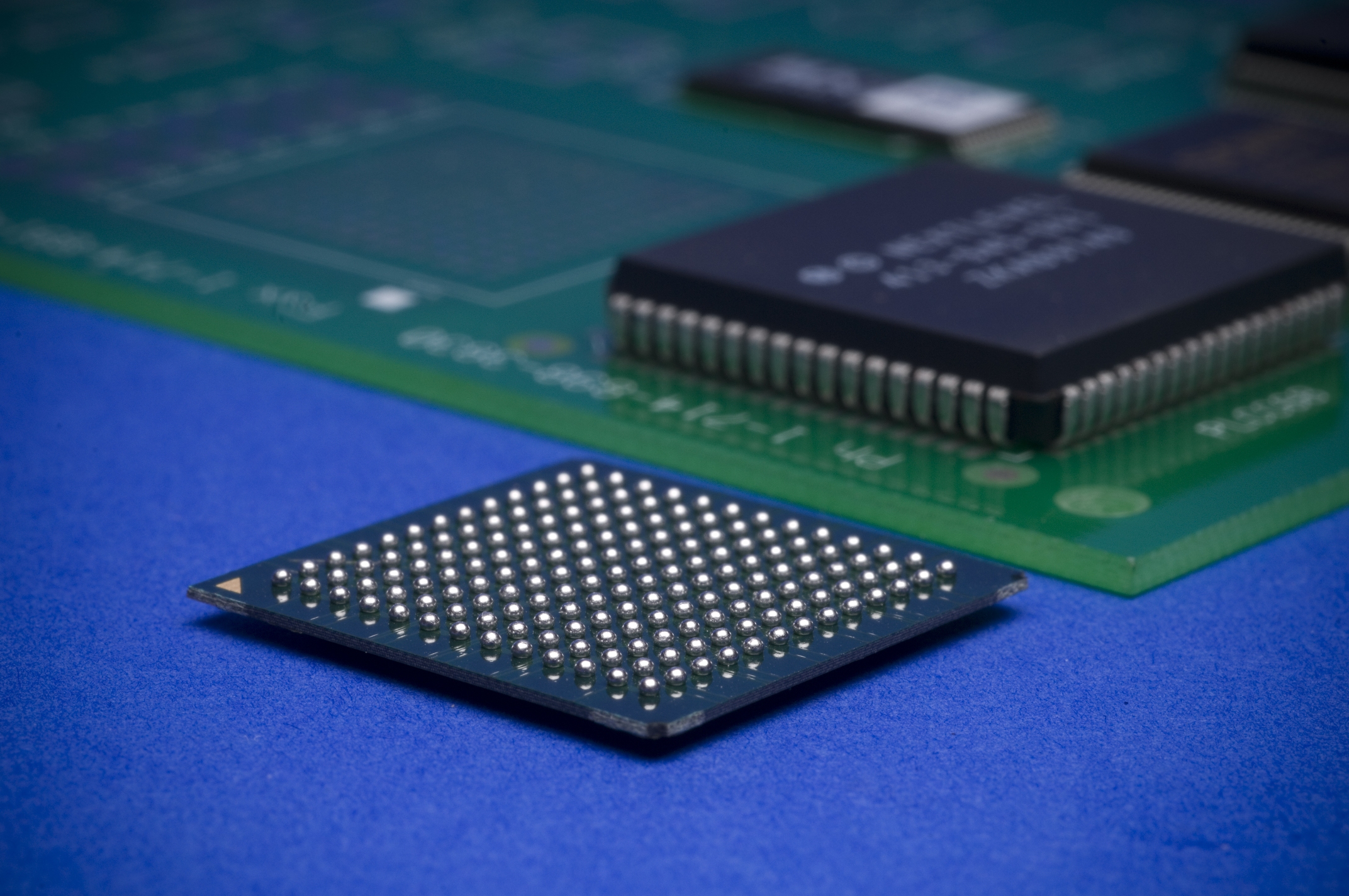
ASE has invested significantly in the research and development as well as in equipment for wafer bumping. The fcFBGA is an overmolded package with solder balls and is available in a high thermal performance package fcFBGA-H produced on substrates in matrix strip format with heat spreader. Wafer bumping is an advanced packaging technique where bumps or balls made of solder are formed on the wafers before being diced into individual chips.
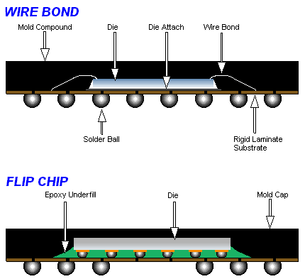
This means these new Flip-Chip packages should be considered as new surface mount devices which. This means these new Flip-Chip packages should be considered as new surface mount devices which. Unlike conventional interconnection through wire bonding flip chip uses solder or gold bumps instead.
The term flip chip describes the method of electrically connecting the die to the package substrate. Your Go-To Provider for a Broad Range of Advanced and Standard Flip Chip Package Solutions. Flip Chip packaging in which the silicon die is directly attached to the substrate using solder bumps instead of wirebonds provides a dense interconnect with the high electrical and thermal performance.
Amkor Flip Chip BGA FCBGA packages are assembled around stateoftheart single unit laminate or ceramic substrates. Therefore the IO pads can be distributed all over the surface of. Disposing at least one chip on the substrate wherein the chip is electrically connected to the substrate.
Flip Chip interconnection provides the ultimate in.
 Study Of Package Warp Behavior For High Performance Flip Chip Bga Sciencedirect
 Flip Chip Packages Stats Chippac Ltd
 Capillary Underfills For Flip Chip Packages Namics Technologies Inc
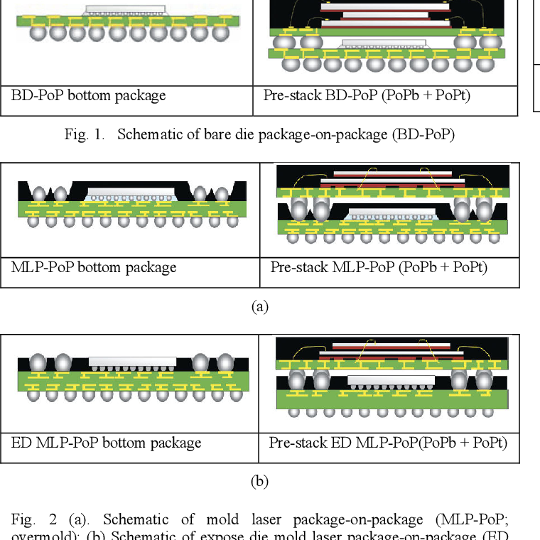 Figure 1 From Advanced Flip Chip Package On Package Technology For Mobile Applications Semantic Scholar
 Flip Chip Article About Flip Chip By The Free Dictionary
 Flipchip Package Overview Anysilicon
 3 Pad Led Flip Chip Cob Led Professional Led Lighting Technology Application Magazine
 Flip Chip Assembly Alter Technology Formerly Optocap
 Flipchip Package Overview Anysilicon
 One Piece Lid High Performance Flip Chip Bga Hpfcbga Package Download Scientific Diagram
 Flip Chip Packaging Amkor Technology
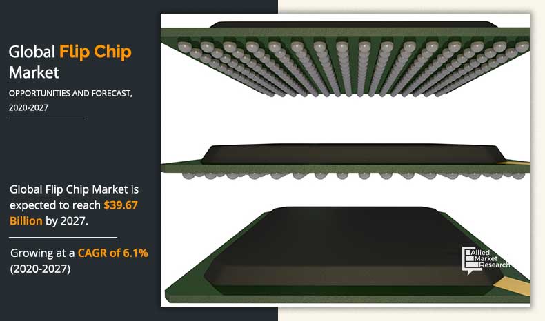 Flip Chip Market Size Share Growth Industry Trends Analysis 2027
 Faraday Technology Corporation Flip Chip Package
 One Piece Lid High Performance Flip Chip Bga Hp Fcbga Package Download Scientific Diagram


Comments
Post a Comment